The world is running short of semiconductor chips—running so short that Subaru has temporarily closed a plant in Japan, 5G network rollouts are delayed, Apple is worried about production hiccups, and new PlayStation 5s are nearly impossible to find. The reason for the shortfall may be plain to see—production slowdowns during the pandemic, compounded by booming demand for consumer technology—but the shortfall itself shows the stunning ubiquity of the chip today, and the dense complexity of the supply chains that produce it.
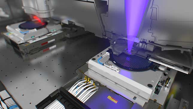
Which makes it all the more remarkable that a single Dutch company sits at the very heart of this $439 billion industry. At its headquarters in Veldhoven, in the Netherlands, ASML assembles photolithography machines, which etch circuit patterns onto chip wafers using low-wavelength light. Other companies make such machines too, but ASML controls more than 60% of the market; in 2019, its revenue was 11.8 billion euros ($13.2 billion). It is also the only manufacturer of the latest, most precise generation of chip-making machines, which uses extreme ultraviolet light (EUV), with a wavelength of 13.5 nanometers—a ten-thousandth the width of a human hair.
It’s difficult to think of another company anywhere that is simultaneously this important and yet this unknown to the public at large. If Veldhoven vanished tomorrow, our version of capitalism—our cellphone-toting, remote-working, Netflix-binging, online-buying, cloud-storing, smart car-driving, Internet-of-Things-ing capitalism—would judder to a halt. ASML isn’t a monopoly, but its market depends upon its technology to a degree that can almost be discomfiting.
ASML provides a window not just into our silicon-chipped world but also into a business that has to ride waves of technological and social change. The company’s singular status places it squarely in the path of any economic or geopolitical turbulence that affects the chip industry. It is, for example, caught between the US and China in their ongoing trade war. And it is, of course, feeling the heat of the chip shortage. To expand its capacity to meet demand would take two years, Peter Wennink, ASML’s chief executive, said. “So we’re just trying to get more people to do more things faster”—that is, to assemble photolithography machines out of their hundreds of thousands of parts, test them, break them down again, fly them to semiconductor plants in Taiwan or South Korea or the US, build them back up, and get them running, so that the plants can try to meet our near-insatiable appetite for chips.
The history of ASML
On the day Frits van Hout joined ASML—May 1, 1984—he arrived at work, only to find that no one knew he’d been hired. The company had just been formed, as a joint venture between Philips and another Dutch firm called Advanced Semiconductor Materials International. “My colleagues asked me: ‘Are you here voluntarily? Did Philips send you here?’ Many people were trying to find a way to get out and go elsewhere,” van Hout, now ASML’s chief strategy officer, said. The first 45 employees were installed in one part of a long factory hall with a leaky roof; within a year, the staff had grown to 200, and the overflow sat and worked in temporary Portakabins.
The first chip bearing integrated circuits was fabricated in 1959, and photolithography—patented just that year—played a significant role in that process. With lenses and mirrors, these machines focused beams of light onto the surface of a silicon wafer to imprint a circuit upon it. This was, essentially, optical work, and through the next couple of decades, as chip manufacturing grew to service a burgeoning computing industry, firms like Canon and Nikon moved into the photolithography business. Philips was a chipmaker and, given its own line of optical technology, wanted to make photolithography machines as well. But, as van Hout said, “if Philips wanted to sell these machines to other chipmakers, they’d say: ‘It looks pretty nice, but how do I trust a fellow chipmaker to give me this stuff?'” Hence the joint venture, van Hout said.
At the time, photolithography was a coarser art than it is today. In each machine, an electricity current heated mercury and generated a plasma, emitting radiation in several wavelengths; the radiation at a wavelength of 436 nanometers was gathered and focused into the required beam of light. At least 10 other companies, including giants like Canon and Nikon, built such machines alongside ASML, and for an upstart, the competition was fierce. “We didn’t know anything about the business side or customers,” van Hout said. “Philips was in big turmoil in the late 1980s, and we were living on the brink of bankruptcy.”
In 1988, ASML was spun off into an independent company. It couldn’t build a factory of its own, to manufacture its components from scratch the way its rivals did. But in the company’s self-crafted origin story, this liability ended up as an advantage—a reason to build strong networks with component suppliers, and to work in a similar modular fashion with its own customers, swapping out parts and units as required. Every few years, the advance of technology allowed companies to work with finer and finer wavelengths of light—365 nanometres, then 248, then 193, and on and on.
But the components also needed vaster and vaster sums of money to develop, and while other firms tried to do it all in-house and faded away, ASML’s suppliers took on a significant part of these costs. Zeiss was already working full time on building better lenses, for instance. For one generation of machines, which required vacuum chambers, ASML could turn to Philips, which knew how to work with vacuums, said Jos Benschop, ASML’s senior vice-president of technology. “It helped,” he added with a grin, “if you were poor.”
How ASML came to dominate its industry
By the early 2000s, several things had changed. The only major competitors remaining were Canon and Nikon, “both not very lean and mean, and ASML was relatively faster,” van Hout said. The internet exploded, and new consumer devices like digital cameras, USB drives and mp3 players all began requiring chips. Around that time, Benschop said, “we put all our eggs into one basket.” Instead of conducting multiple research programs into the photolithography technology of the future, ASML funded only its EUV drive.
For a while, that didn’t feel like the right bet. Progress towards the EUV stumbled again and again. The machines needed to get lasers to hit every one of 50,000 drops of molten tin released each second, so that the resultant plasma would generate 13.5 nanometre light. The development got so costly and complicated that ASML invited some of its customers—Intel, Samsung, the Taiwan Semiconductor Manufacturing Company (TSMC)—to buy stakes in itself, so that the money could be used to fund research.
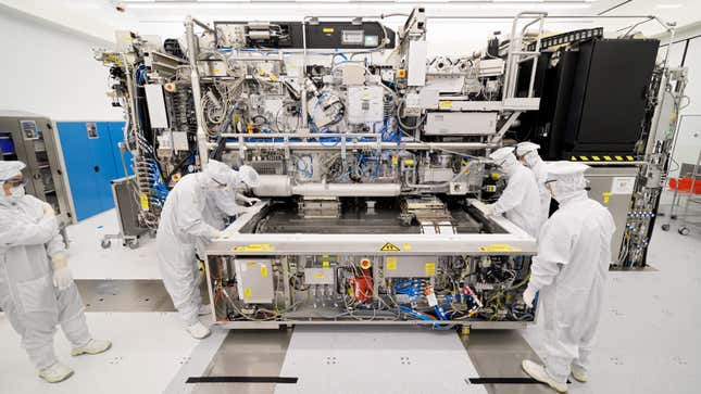
The first EUV prototype was shipped in 2010, and the first production-ready machines in 2016. Each EUV weighs 180 tons, takes 17-18 weeks to assemble, and costs more than $120 million; last year, out of the 258 photolithography systems it sold, 31 were EUVs. The disassembled parts of an EUV fill 150 crates, and ASML needs three Boeing 747s to transport them to its customers. In the plants where it spits out chips, ASML teams have to be on site all the time to maintain, repair and upgrade them. It’s an expensive machine to run as well; one analyst estimated that companies need to invest $1 billion in facilities just to begin using an EUV to produce chips at high volume.
But as the most significant leap forward from the previous technology, it became the way for chipmakers to gain an edge. Samsung and TSMC used EUV machines, said Velu Sinha, a partner in Bain & Company’s technology practice, “whereas Intel announced recently that one of its challenges was that it hadn’t relied on EUV much at all.” ASML sells hundreds of photolithography machines every year, and most of them aren’t EUVs; older machines are still required to make chips that don’t have to be blazingly fast. But by 2025, ASML expects that three-quarters of its revenue will come from EUVs. More crucially, it will have its EUV expertise to build towards the next generation of photolithography technology, expanding its near-monopoly of its terrain.
The geopolitics of semiconductors
The world’s largest consumer of semiconductor chips is China; in 2020, the country imported 543 billion chips, worth around $350 billion. Its state-owned chipmaker, SMIC, was founded in 2000. “Back then, the manufacturing didn’t have to be as precise, so it didn’t matter if you didn’t have the most rigorous clean rooms or if a truck rolling down the road outside shook the building minutely,” Sinha said.
But over the past decade or so, the processes have become much more exacting. At the same time, Sinha said, the US government grew worried about what China might use cutting-edge chips for, and what surveillance technology it might install on any chips it sells to the world. “The concern was, if you allow China to go and make chips at scale using an EUV, those chips would be impossible to scrutinize with all their billions of transistors on them,” Sinha said. Under US pressure, chipmakers were restricted from selling their products to Huawei. Along similar lines, ASML’s EUV was placed on the Wassenaar list, a multilateral regime that controls the export of several critical technologies to non-member states such as China.
It doesn’t take any great insight into the human psyche to discover what Wennink, ASML’s CEO, thinks of not being able to sell to the world’s biggest market. He knows that behind the ban on selling EUVs to China is not just a worry about national security but also an act of economic one-upmanship—a desire to keep China dependent on non-Chinese vendors. Most military applications don’t even need cutting-edge chips from EUVs, he argued. They can work just fine with older chips. “And the argument we make to governments is that…our equipment is part of a production system for products that are so multifunctional and general purpose,” Wennink said. “They help process medical data. Or traffic data… You try to educate governments that a sanction will slow innovation, and costs will go up.”
Photolithography today is so complex that it’s difficult to set up a company from scratch to make these machines. Still, the possibility always exists that China will seed and grow photolithography machine manufacturers—becoming not just self-sufficient in chips but competitive with ASML. If this worries Wennink, he doesn’t express it. Sinha too thinks that the sanctions represent just a five or ten-year delay in China’s semiconductor ambitions. “The government just put an absurd $30 billion into this in its latest economic plan to catch up,” he said. “It isn’t Game Over—it isn’t that China will never get there.”
Meanwhile, it isn’t as if ASML is hurting for business at the moment. Our modern lives are so chip-dependent that eventually more foundries will emerge in Asia, the US, and Europe, Sinha said. And if ASML bides its time, the geopolitical and economic currents will change, such that the company isn’t caught in their crossflow and can sell its machines anywhere it pleases. Wennink knows this too, and he hopes that the sanctions will drop away at some point. “It would have frustrated me if I was 20 years younger. Now I just live with the reality.”